- v50 information can now be added to pages in the main namespace. v0.47 information can still be found in the DF2014 namespace. See here for more details on the new versioning policy.
- Use this page to report any issues related to the migration.
Difference between revisions of "User:Jong/Dwarven Computer"
m |
m |
||
| Line 555: | Line 555: | ||
==External links== | ==External links== | ||
*[http://docs.google.com/Doc?docid=0AdISzBuNg6ZWZGd0d2t4YjlfMjJ0ejlzc2dnaA&hl=en GoogleDocs Design Manuscript] | *[http://docs.google.com/Doc?docid=0AdISzBuNg6ZWZGd0d2t4YjlfMjJ0ejlzc2dnaA&hl=en GoogleDocs Design Manuscript] | ||
| − | *[http://www.bay12forums.com/smf/index.php?topic=49641.0 Bay12 Forums thread] | + | *[http://www.bay12forums.com/smf/index.php?topic=49641.0 Bay12 Forums thread] - Includes discussion on modifications and testing results |
*[http://mkv25.net/dfma/map-8269 Map at DF Map Archive] | *[http://mkv25.net/dfma/map-8269 Map at DF Map Archive] | ||
*[http://dffd.wimbli.com/file.php?id=1929 Save File at DF File Depot] | *[http://dffd.wimbli.com/file.php?id=1929 Save File at DF File Depot] | ||
Revision as of 09:38, 30 April 2010
This page documents the design of my Dwarven Computer. A number of designs were modified for the final implementation.
Adapted from my GoogleDocs manuscript
Notes
Toggled gear assemblies are designed as though they are off in when untriggered. However they are constructed in the on position. This means that you need to build and link a lever to toggle it to the off state.
Power sensor (output device)
 # %>^ #
~ ~ ~ ~#      Power sensor side view
In order to do useful things, such as toggling gears assemblies, opening doors, etc., mechanical power signals need to be converted to a trigger signal. There are only 2 trigger signal generators in dwarf fortress. One is the lever, which cannot be linked to machine power. The other is a pressure plate, which can.
The basic operation of this component is simple. Power operates the pump, pushing water over the pressure plate, generating a signal. When the pump is not powered, the water drains, switching the pressure plate off after at least 100 steps.
The smooth operation of this unit depends on several factors: 1. Adequate supply of water in the input tile so that the pump can maintain 7/7 or 6/7 water levels on the pressure plate. Can be done by providing more water tiles adjacent to the input tile. 2. Fast drainage to minimize the time needed for the plate to switch off. Just make sure that the level below the pumps is not completely full. 3. Since the minimum recovery time of the pressure plate is 100 steps, it can take a good long time for a 0-bit to reach the end of a chain of output units.
Design for a memory cell for use in registers/memory unit
###
#H#
#^#PRoO
#%#
#%WIP
#~#
###
This design is based on plans found at User:SL/Logic_Gates on the wiki. For this design, the write-in signal is linked to gear W and hatch H, while the read-out signal is linked to gear R. Gear o is linked to the pressure plate ^ and represents the state of the cell. Big O represents to output signal and I represents the input signal. P represents a power source. The hatch prevents the water from draining thus preserving the data.
In order to act as a memory cell, this unit must do 3 things: 1. Output its state when told to read-out 2. Change state to match an input when told to write-in 3. Maintain its state when not told to do anything
Let's check this by examining the operation of this unit.
| R | W | I | State | O |
|---|---|---|---|---|
| 0 | 0 | Ignored | Unchanged | 0 |
| 1 | 0 | Ignored | 0 | 0 |
| 1 | 0 | Ignored | 1 | 1 |
| 0 | 1 | 1 | 1 | 0 |
| 0 | 1 | 0 | 0 | 0 |
| 1 | 1 | 1 | 1 | 1 |
When both read and write are turned on, the device will act as a power sensor for the input. This could be a problem if the input and output are linked.
One point of concern is that the unit may not contain sufficient water to trigger the plate because the amount of water in the square above the hatch may not be 7 when it closes.
The plate could be set to trigger at a lower threshold, which would slightly slow down response time, or a door could be used instead of a hatch and the unit extended by one tile to provide space for the drain. This would have the downside of destroying some water after every write operation.
Another method is to use another pump to drain the water from the holding tile. This pump will only activate when W is 1 and I is 0.
Computer registers
The dwarven computer prototype is going to have an 8-bit instruction length, a 3-bit operon and a 5-bit address space. Why? The best reason for this is that other designs of Very Simple Computers (VSC) on the Internet are also only 8-bit and I am basing the design of the prototype dwarven computer off several of them. Naturally a bigger computer is better in many ways but the current goal is to produce an operational one. Now its not clear to me why a VSC shouldn't be smaller, but I suppose it doesn't matter.
8-bit words need 8-bit registers. Fortunately this just means stacking 8 memory units up and making sure they receive the same read/write signals.
The lines in the diagram don't actually represent physical connections but imaginary ones. After all, the write signal must be sent remotely.
Now we consider the most compact designs for such an array. Let us assume that the output signals will be sent remotely. For clarity, the arrays ought to be rectangular.
##### ##### ##### ##### ##### ##### ##### #####
#H#.# #H#.# #H#.# #H#.# #H#.# #H#.# #H#.# #H#.#
#^#^# #^#^# #^#^# #^#^# #^#^# #^#^# #^#^# #^#^#
#%#%# #%#%# #%#%# #%#%# #%#%# #%#%# #%#%# #%#%#
W%`%o W%`%o W%`%o W%`%o W%`%o W%`%o W%`%o W%`%o
I~`~RPI~`~RPI~`~RPI~`~RPI~`~RPI~`~RPI~`~RPI~`~R
P`P
Note that the O is omitted since it was a placeholder for the output device.
Not all registers in the computer are 8 bit registers. For example the memory address register is 5 bits.
Memory unit
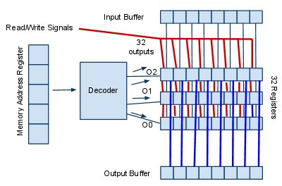
Since there are only 5 bits of address space, I only need 256 memory cells. It should be fine if I don't use complicated column and row addressing schemes. I shall simply have 32 8-bit registers sticking somewhere. In order for the memory unit to work, I need a decoder to change the 5-bit address into 32 outputs. This will enable the memory unit to read and write from any register. I guess this makes it random access memory.
Decoder
This type of decoder is called an n to 2^n decoder, since it converts n inputs into 2^n outputs, in this case 5 to 32(2^5).
To illustrate the design for this unit, let us consider a simpler example where n=2. There will be 2 binary inputs which will be converted into 4 unique outputs, 1 for each memory address.
Here is the truth table for the operation:
| 2^0 (1) | 2^1 (2) | O0 | O1 | O2 | O3 |
|---|---|---|---|---|---|
| 0 | 0 | 1 | 0 | 0 | 0 |
| 1 | 0 | 0 | 1 | 0 | 0 |
| 0 | 1 | 0 | 0 | 1 | 0 |
| 1 | 1 | 0 | 0 | 0 | 1 |
Now let us examine the implementation into the dwarfputer. Remember that gear assemblies are toggleable. I can implement a NOT operation by simply reversing the default state of a triggered gear (which is OFF in this system).
Let us represent the 2^0 gear as A when it is default OFF and as a when it is default ON, and represent the 2^1 gear as B and b. O0 to O3 represent output devices.
P  P  P  P
a  A  a  A
b  b  B  B
O0 O1 O2 O3
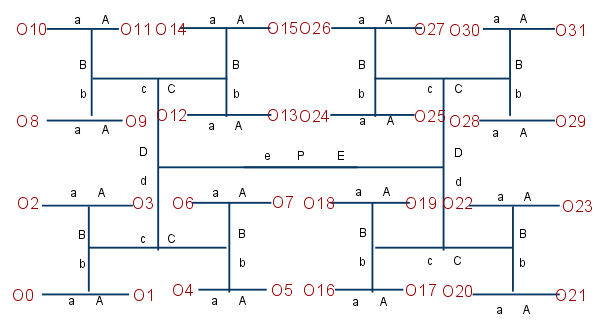
This is the easiest to understand implementation. Looking at O0, we see that O0 is powered only when a and b are active. This corresponds to the state when 2^0 and 2^1 are both 0. Examining all the devices reveals that this arrangement obeys the truth table detailed above. Further examination would reveal that this arrangement also follows a pattern. Basically, the full set of columns represent every single possible combination of a, A, b, and B. Therefore we can easily see how to expand this system to n=5.
However, this implementation is not the most efficient one. I can also arrange the gears like so:
O3A AO1
  BPb
O2a aO0
This arrangement uses 7 gears while the first arrangement uses 12 gears (including power gears). I put B and b closest to the power supply to obtain an orderly arrangement of O0 to O3 although this isn't strictly necessary.
Schematically this arrangement looks like this:
Which is just some sort of tree diagram. I can easily expand this to n=5 which is what I want.
I drew this diagram in rectangular form so that I can better see how to construct the decoder. The outputs of the decoder will be in a 4x8 grid. Since the output units are longer in one direction than the other, I will align their long axis along the short axis of the diagram. It is probably best to place all the mechanisms for the decoder in the level above the outputs.
Memory unit registers
The registers in the memory unit need some modification to work correctly. Only the register indicated in the memory address register ought to respond to read write signals. Therefore each of the 32 registers needs to be connected to one of the outputs from the decoder.
In this example, the register only responds when 00000 is in the memory address register.
##### ##### ##### ##### ##### ##### ##### #####
#H#.# #H#.# #H#.# #H#.# #H#.# #H#.# #H#.# #H#.#
#^#^# #^#^# #^#^# #^#^# #^#^# #^#^# #^#^# #^#^#
#%#%# #%#%# #%#%# #%#%# #%#%# #%#%# #%#%# #%#%#
W%`%o W%`%o W%`%o W%`%o W%`%o W%`%o W%`%o W%`%o
I~`~RCI~`~RCI~`~RCI~`~RCI~`~RCI~`~RCI~`~RCI~`~R
CP`P`P`P`P`P`P`P`PC
C in this diagram represents the output O0. I believe this is called the chip select signal in real computers.
It may be possible to wire the decoder directly to the power supply of the memory, which would remove the need for an output device.
Memory unit architecture
Right, I based the design of the memory unit off a java applet simulator I found on the Internet.
What this diagram is supposed to illustrate is that ALL the memory cells are linked to respond to the same read-out signal and the same write-in signal. Similarly, all the corresponding cells respond to same input, and all output to the same place. However, they will do none of these things unless they get a signal from the decoder, and only one register will get the signal as indicated in the memory address register.
Now the input and output buffers shown here may not be in the final blueprints, depending on the design of the rest of the computer.
Machine language design
The machine language is the set of instructions the computer will be able to execute. What these instructions are will define the design of the remaining components. For example, the Arithmetic Logic Unit needs to be able to perform the various operations listed in these instructions.
Ideally this language should be complete, that is, any function can be simulated as a combination of these instructions. I also want to be as simple as possible, to minimize the complexity of the ALU. It is worth restating that I am basing the overall design for the computer on a design for a VSC off the Internet.
Since the opcode for this computer is 3-bits long, there can only be 8 instructions.
| Opcode | Function | Operand |
|---|---|---|
| 000 | Load Accumulator from memory (indirectly) | Memory Address |
| 001 | Store Accumulator to memory | Memory Address |
| 010 | Add | Memory Address |
| 011 | Subtract | Memory Address |
| 100 | Jump to address if accumulator is not negative | Memory Address |
| 101 | Binary shift left (*2) (input 0 as LSB) | Memory Address |
| 110 | Binary shift right (/2) (retain MSB) | Memory Address |
| 111 | Halt | None |
Arithmetic Logic Unit (ALU)
Now I know that the ALU needs to be able to perform 4 functions: Add, subtract, shift left and shift right. The unit needs to do one of these functions based on one of 4 input signals it may receive.
The ALU will receive 2 8-bit inputs and produce 1 8-bit output. It will require 3 systems, the adder-subtractor, bitshift left and bitshift right. These systems would be integrated to form the ALU.
Half adder
While there are existing dwarven adder designs out there, they do not come with schematics detailing the links between their components. Therefore I feel the need to design from scratch.
A simple half adder would take 2 inputs, and produce an output and an overflow output called a carry.
| A | B | C | O |
|---|---|---|---|
| 0 | 0 | 0 | 0 |
| 1 | 0 | 0 | 1 |
| 0 | 1 | 0 | 1 |
| 1 | 1 | 1 | 0 |
Carry out circuit C==ABP
                      aBP
Output circuit     O==o
                      bAP
                 C===A
Combined circuit    aBP
                 O==obA
This schematic shows a dwarven half adder that obeys the above truth table. In this diagram, the o represents a normal gear assembly and = represents axles. This design rests on the assumption that axles do not receive power except from their end tiles. It also takes advantage of the assumption that a matched pair of gears will not transmit information across their connection (here it is the B and b gear)
I believe this design uses the minimum number of gear assemblies, although I am not sure.
Full adder
In order for an adder to work properly, it must also receive the carry bit in addition to the 2 inputs. Ultimately, even the first adder in the final adder-subtracter must be able to receive a carry bit to operate successfully, which is why I didn't draw up a full plan for the half adder.
| A | B | C (carry in) | O2 (carry out) | O1 |
|---|---|---|---|---|
| 0 | 0 | 0 | 0 | 0 |
| 1 | 0 | 0 | 0 | 1 |
| 0 | 1 | 0 | 0 | 1 |
| 1 | 1 | 0 | 1 | 0 |
| 0 | 0 | 1 | 0 | 1 |
| 1 | 0 | 1 | 1 | 0 |
| 0 | 1 | 1 | 1 | 0 |
| 1 | 1 | 1 | 1 | 1 |
PB
CAo==O2       Carry Out Circuit
oBo
o=o=o=o==O1   Output Circuit
C c c C
B b B b
A A a a
P P P P
    O1 O2     Combined Circuit
 oo=oo |
 Cc cC oo
 Bb BbBAB
PAo oaPCo
Now that looks pretty monstrous. Undoubtedly the arrangement of gears could be changed here and there depending on the exact dimensions you need the array to be, but hopefully this diagram illustrates methods that can be used to minimize the complexity of the device. Note that where there are adjacent identical gears directly connected to the power source, one of them can be replaced by an ordinary gear, which will remove a linking task for that gear.
` oCBAPocbo #####|#.#.#`ocBo#^#^#` `ooCba Hypothetical implementation #%#%#` `oBP`%`%`oAC `~`~`oBo`` lvlz lvlz+1
The above diagram details a hypothetical implementation for a full adder. The `s represent the shadow of the mechanisms above and below the level. The left power sensor produces the output signal while the right power sensor produces the carry signal to be relayed to the next adder. The total footprint of the unit is 6x9. In an array, the units can overlap one tile so the total footprint of an 8-bit adder would be 41x9. Maximum operational power draw is 131x8(1048) units of power.
8-bit ripple-carry adder-subtracter
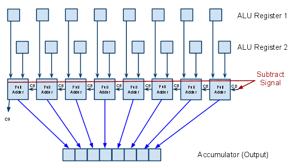
In order to build a full 8-bit adder-subtracter, all you need to do is to stack up 8 full adders next to each other and ensure that all the gears have been linked to the appropriate plates.
Now to get the adder-subtracter to subtract, all you have to do is to link up every single A and a (or B and b) gear assembly to the pressure plate sending the subtract signal. When the signal is sent, all the gears linked to a register will toggle. This will have the effect of inverting whatever input the register is sending. Finally the signal also needs to activate the carry in gears in the first adder, which will have the effect of adding 1 to the resulting sum (difference), giving the correct answer in two's complement representation.
Carry-look-ahead adder
I did some research into carry-look-ahead adders to see if it was worth implementing. Carry-look-ahead adders are faster than ripple-carry adders as ripple carry adders have to wait for the carry bit to 'ripple' through the chain of adders before getting the correct result. This is most significant for users of fluid logic, as fluid logic adders need to wait n*100 steps (n being the number of bits) for the carry to ripple all the way to the end. (Floodgates and bridges have a 100 step delay before activating or deactivating)
I found that I could easily design a carry-look-ahead adder using mechanical logic that calculates the carry in bit for all bits in a single step. I would also like to point out that real carry-look-ahead adders are more complicated because they don't have teleporting switch signals.
Firstly, looking at the carry-out circuit for the full adder, I see that not only can it exist independently from the sum circuit, the C gear is directly attached to the power source. I can take advantage of this by separating the carry bit calculation circuits from the adder and attaching them to each other like so.
Then for the summing part of the adder, I simply build only the output circuit, which I can now simplify like this
    O1     Output Circuit
 oo=oo
 Cc cC
 Bb Bb
 oAPao
Or I can make it long instead of square so that it will tile better with the output buffers.
   O1
   |
oBCoCbo
AbcocBa
P     P
I could construct these directly above the output buffers and they would all tile a lot better. Not only that, it fits almost perfectly within the footprint of a bank of output buffers. There is also no cost of increased complexity, only spatial separation between the summation unit and the carry unit, plus providing all the advantages of the carry-look-ahead system.
Since this system is superior in all ways to the ripple-carry system, this will be the one going into the final dwarven computer.
Bitshifting operations
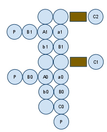
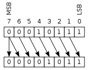
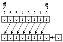
Setting up a bitshifting operation is relatively simple. I simply wire the inputs directly into slightly different outputs as illustrated in the following diagrams (source: Wikipedia http://en.wikipedia.org/wiki/Bitwise_operation#Arithmetic_shift).
Ideally all these operations would be linked into the same bank of output buffers in the assembled ALU, which will be the subject of the next section.
ALU architecture
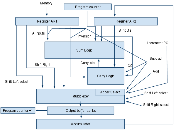
This diagram illustrates the various signals moving around the ALU. I decided that I ought to dragoon the ALU into incrementing the program counter as well, but I'm not sure whether that will work or not. We'll see in the later sections.
I defined the inputs from AR1 to be A since there are fewer A and a gears in the current designs and they all have to be toggled by the subtract signal. The operations listed on the right are signals generated by the control unit and they tell the ALU which operation to perform and transfer to the output buffer banks. The component critical to this function is the multiplexer.
The concept of the multiplexer is quite simple, suppose I had 2 inputs I and J, and I wanted to choose which one to pass based on signals Q and R, I would have to build something like this
PQIoJRP
   |
   O
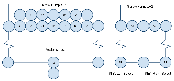
Adding a multiplexer onto the output circuit would require an additional z-level if the tiling efficiency is to be maintained.
This diagram illustrates a hypothetical implementation of the multiplexer, as well as the bitshifting logic. I don't think I need a support axle on z+2 as it should be supported by O1.
Bus design
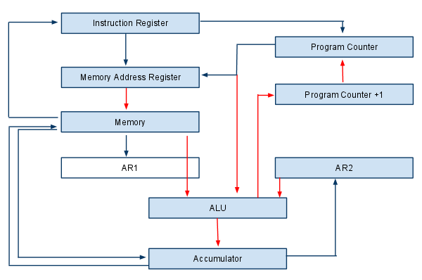
I've decided to ditch the plan for a bus, which would have been the conduit for data transfers between registers throughout the computer. Initially there were 2 methods, one had a output buffer attached to the end of the bus while the other the bus directly supplied power to the inputs of the appropriate registers.
Method 2 would not work on memory cells that used an active pump for bit-clearing. Method 1 would have worked but the output buffers had to be overwritten every step and that could cause cascading delays throughout the computer. Since this computer is relatively simple, I opted for hard wiring everything instead.
This diagram illustrates the data transfers that occur throughout the computer. The red arrows depict confirmed hard-wired connections, while the blue arrows would have been routed through a bus. I've decide AR1 is superfluous so I got rid of it. As you can see, each register has at most 2 inputs or 2 outputs going through the bus, so hardwiring is feasible.
Timing circuit
Before the computer can execute its instructions, it needs to perform some operations first.
- Transfer the contents of the accumulator to AR2. Dump instruction register and memory address register.
- Transfer the program counter to the memory address register. Also, activate the program counter incrementation system in the ALU and transfer the results into program counter +1.
- Load the data from memory at the specified address into the instruction register.
- Transfer the data from program counter +1 to the program counter. Also, dump the memory address register
- Load the last 5 digits of the instruction register into the memory address register. Also, dump program counter +1.
- Execution (write accumulator, memory or program counter, read instruction register, memory, AR2)
There needs to be a 100 step delay from the time a memory cell is written (or dumped, if it is pre-dumped) and when it is read, or it may cause cascading delays. The writing process is practically instantaneous, but 100 steps are needed before the correct result can be read if the memory was not cleared to begin with. Of course this point is entirely moot if the computer is running automatically, in which case every step will last at least 100 steps anyway and the prime consideration is to ensure that every step can be performed in 100 steps.
Oscillator
A typical mechanical oscillator is unsatisfactory because it will usually be sending out 2 on signals at once, one from the pressure plate the water is on and the other from the pressure plate waiting to reset.
0%%6%%0%%5%%0%%4
%              %
%              %
1%%0%%2%%0%%3%%0
This diagram shows a 12 step 6 signal oscillator. At the locations marked 0, there are no pressure plates. A lever operates the mechanism. When the lever is in the ON position, the #%%0 pumps activate, and when the lever is in the OFF position, the 0%%# pumps activate. The oscillator can also be fully automated by using the pressure plates themselves to replace the lever function. The oscillator's power supply also needs to be cut if a halt signal is received from the control unit.
Oscillator link table
- Read accumulator, write AR2, write IR, write MAR
- Read PC, write MAR, activate ALU (adder select, C0=1), write PC+1
- Read MEM, read MAR. activate decoder, write IR
- Read PC+1, write PC, write MAR
- Read IR, write MAR, write PC+1
- Execution (read IR, turn on control unit)
A dump operation can be performed by telling the memory register to write when its linked inputs are inactive, effectively writing 0s.
Control unit
The control unit can be implemented simply as a 3-8 decoder with appropriately linked pressure plates. The execute signal controlled gear assembly is located at the root of the decoder.
Control unit link table
- O0. Read memory, read MAR, activate decoder, write accumulator, select transfer
- O1. Read accumulator, write memory, read MAR, activate decoder
- O2. Read memory, read MAR, activate decoder, read AR2, Send Add signal to ALU (adder select), write accumulator
- O3. Read memory, read MAR, activate decoder, read AR2, Send Subtract signal to ALU (adder select, C0=1, invert input A), write accumulator
- O4. Read IR, write PC if ACC7=0
- O5. Read memory, read MAR, activate decoder, Send Shift left signal to ALU (SHL select), write accumulator
- O6. Read memory, read MAR, activate decoder, Send Shift right signal to ALU (SHR select), write accumulator
- O7. Cut power to oscillator.
See also
External links
- GoogleDocs Design Manuscript
- Bay12 Forums thread - Includes discussion on modifications and testing results
- Map at DF Map Archive
- Save File at DF File Depot


